The only wafer fab AFM with automatic defect review
Low Noise, High Throughput Atomic Force Profiler
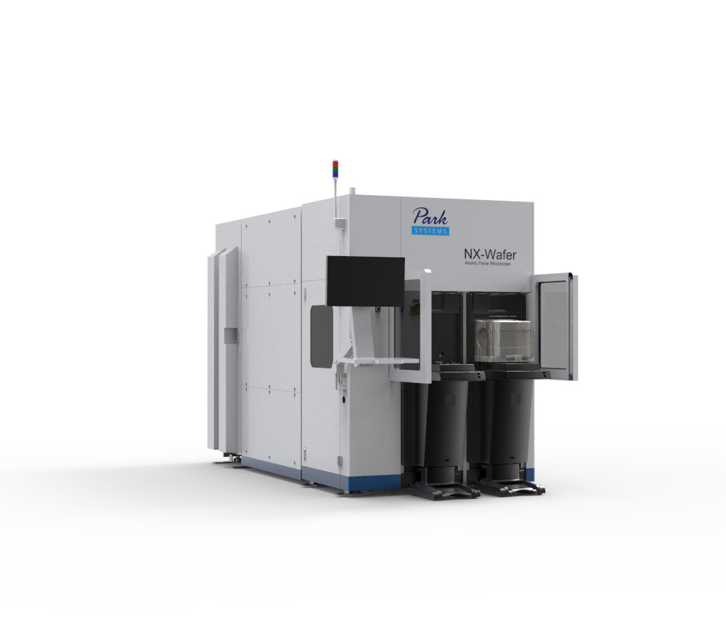
Park NX-Wafer is the industry’s leading automated AFM metrology system for semiconductor and related fabrications. It provides wafer fab inspection and analysis, automatic defect review for bare wafers and substrates, and CMP profile measurements. Park NX-Wafer has the highest nanoscale surface resolution with sub-angstrom height accuracy, scan after scan with negligible tip to tip variation and preserved tip sharpness unmatched by others.
Park NX-Wafer with its automated system features including auto tip exchanger, live monitoring, target positioning without reference marks and auto analysis makes the best semiconductor AFM tool in the industry.
Low noise atomic force profiler for more accurate CMP profile measurements
-
Sub-Angstrom surface roughness measurements with extreme accuracy and negligible tip-to-tip variation
-
Fully automated AFM solution for defect imaging and analysis
-
A fully automated system with auto tip exchange, robot wafer handler
-
Capable of scanning 300 mm wafers
Park NX-Wafer Specifications
System Specification:
Motorized XY stage
+ 200mm : travels up to 275 mm × 200 mm, 0.5 µm resolution
+ 300mm : travels up to 400 mm × 300 mm, 0.5 µm resolution, 1 µm repeatability
Motorized Z stage
+ 25 mm Z travel distance,
+ 0.08 µm resolution, < 1 µm repeatability
Motorized Focus Stage: 9 mm Z travel distance for on-axis optics
Sample Thickness Allowance: up to 20 mm
Full scan range Z run-out: < 2 nm, repeatability < 1nm
COGNEX Pattern Recognition: pattern align resolution of 1/4 pixel
Scanner Performances:
XY Scanner
+ 100 µm × 100 µm (Large mode)
+ 50 µm × 50 µm (Medium mode)
+ 10 µm × 10 µm (Small mode)
+ Single-module flexure XY scanner with closed-loop control
XY Scanner Resolution
+ 0.15 nm (Large mode)
Z Scanner Range
+ 15 µm (Large mode)
+ 2 µm (Small mode)
Z Scanner Resolution
+ 0.016 nm (Large mode)
+ 0.002 nm (Small mode)
Z Scanner Detector Noise
+ 0.03 nm, rms (typical)
AFM and XY Stage Control Electronics
ADC
+ 18 channels
+ 4 high-speed ADC channels
+ 24-bit ADCs for X,Y and Z scanner position sensor
DAC
+ 17 channels
+ 2 high-speed DAC channels
+ 20-bit DACs for X,Y and Z scanner positioning
Compliances: CE - SEMI Standard S2/S8
Vibration, Acoustic Noise, and ESD Performances
+ Floor Vibration: < 0.5 µm/s (10 Hz to 200 Hz w/ Active Vibration Isolation System
+ Acoustic Noise: >20 dB attenuation w/ Acoustic Enclosure
Facility Requirements:
+ Room Temperature (Stand By): 10 °C ~ 40 °C
+ Room Temperature (Operating): 18 °C ~ 24 °C
+ Humidity: 30% to 60% (not condensing)
+ Floor Vibration Level: VC-D (6µm/sec)
+ Acoustic Noise: Below 65 dB
+ Pneumatics:
+ Vacuum : -80 kPa
+ CDA (or N2): 0.7 MPa
+ Power Supply Rating: 208V - 240 V, single phase, 15 A (max)
+ Total Power Consumption: 2 KW (typical)
+ Ground Resistance: Below 100 ohms
Options:
Long Range Sliding Stage
• 200mm : 10 mm
• 300mm : 25 mm (optional 10 mm or 50 mm)
Automatic Tip Exchange (ATX)
Automatic Tip Exchange performs fully automated tip exchanges in order to seamlessly continue automated measurement routines. It automatically calibrates cantilever location and optimizes measurement settings based on measurements of a reference pattern. Our novel magnetic approach to the tip exchange yields a 99% success rate, higher than the traditional vacuum techniques.
Automatic Wafer Handler (EFEM or FOUP)
The XE-3DM can be further customized by adding an automatic wafer handler (EFEM or FOUP or other). The high-precision, nondestructive wafer handler robot arm fully ensures XE-3DM users to receive fast and reliable wafer measurement automation.
Ionization System
Ionization system effectively removes electrostatic charges. It ionizes the charged objects and is very reliable since the system always generates and maintains an ideal balance of positive and negative ions without causing any contamination to the surrounding area. It also reduces the accidental electrostatic built-in charge that may occur during sample handling.
High productivity and powerful features for inline wafer-fab metrology
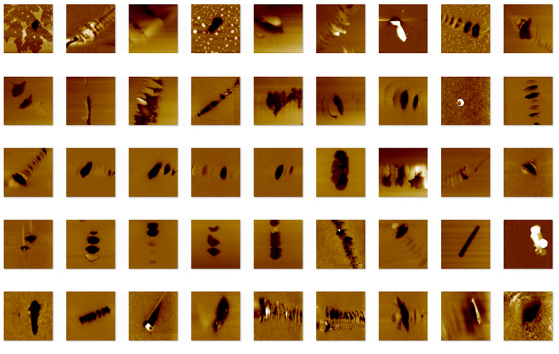
Automatic Defect Review for Bare Wafers and Substrates
The new 300mm bare wafer ADR provides a fully automated defect review process from transfer and alignment of defect maps to the survey and zoom-in scan imaging of defects that uses a unique remapping process that does not require any reference marker on a sample wafer. Unlike SEM which leaves square-shaped destructive irradiation marks on defect sites after its run, . the AFM-based defect review enables non-destructive 3D imaging of defects as small as a few nanometers. The linkage between a defect inspection tool and the AFM is carried out by advanced coordinate translation with enhanced vision technique. Since it is fully automated, it does not require any separate steps to calibrate the stage of the targeted defect inspection system, increasing throughput by up to 1,000%.
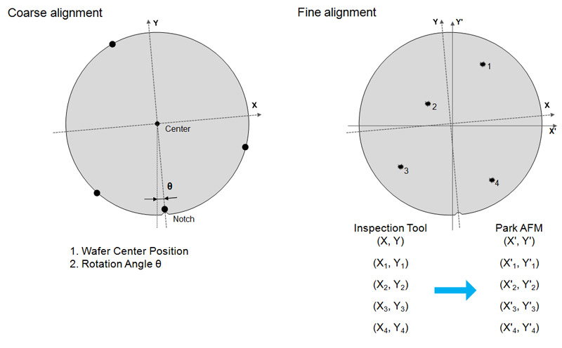
Automatic Transfer and Alignment of Defect Maps with Enhanced Vision
By utilizing Park's proprietary coordinate translation technique, the new Park ADR AFM can accurately transfer the defect maps obtained from a laser-scattering defect inspection tool to a 300mm Park AFM system. This technology does not require any separate step to calibrate the stage of the targeted defect inspection system and allows full automation for high throughput defect imaging.
Automated Search & Zoom-in Scan
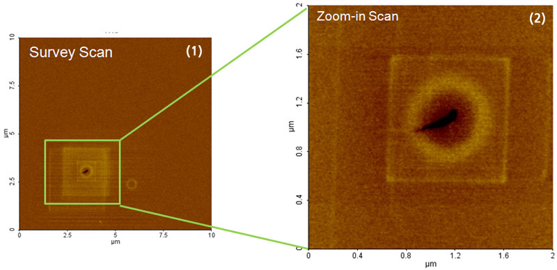
The defects are imaged in two steps;(1) a survey imaging, either by AFM or enhanced optical vision, to refine the defect location, then (2) a zoom-in AFM scan to obtain a detailed image of the defect, presenting automatic analysis of the defect type and the subsequent defect dimensions. .
Long Range Profiling for CMP Characterization
Planarization is the most important step in the back-end processes where metals and dielectric materials are used. Both local and global uniformity after chemical mechanical polishing (CMP) affect the yield of chip manufacturing significantly. Accurate CMP profiling is a critical metrology necessary to optimize process conditions for best planarity and improve production yield.
Combining Park NX-Wafer with a sliding stage provides a long range profiling capability for CMP metrology. Due to the unique scanner design of Park's automated AFM, the combined system provides very flat profiling and there is no need for complex background subtraction or calibration after each measurement. The Park NX-Wafer enables unprecedented CMP metrology of both local and global planarity measurements including dishing, erosion, and edge-over-erosion (EOE).
Sub-Angstrom Surface Roughness Control
Semiconductor suppliers are developing ultra-flat wafers to address the ever-increasing need for shrinking device dimensions. However, there has never been a metrology tool capable of providing accurate and reliable measurements for the sub-Angstrom roughness of these substrate surfaces. By delivering the industry's lowest noise floor of less than 0.5 Å throughout the wafer area, and combining it with True Non-Contact Mode™, the Park NX-Wafer can make accurate, repeatable, and reproducible sub-Angstrom roughness measurements for the flattest substrates and wafers with minimized tip-to-tip variation. Very accurate and repeatable surface measurements can be obtained even for the long-range waviness measurement of scan sizes up to 100m x 100m.
High-Throughput Wafer-Fab Inspection and Analysis
• Automatic tip exchange with 99.9% success rate and minimum tact time
• Equipment Front End Module (EFEM) for automatic wafer handling
• Cleanroom compatibility and remote control interface
• Automatic data acquisition and analysis of trench width, depth, and angle measurements
Park NX-Wafer features
Long Range Sliding Stage
The long range profiler is an essential component of Atomic Force Profilometry (AFP) and comes with a dedicated user interface for the automated CMP profiling and analysis.
• 200mm : 10 mm
• 300mm : 25 mm (optional 10 mm or 50 mm)
100 µm x 100 µm Flexure-Guided XY Scanner with Closed-loop Dual Servo System
The XY scanner consists of symmetrical 2-dimensional flexure and high-force piezoelectric stacks that provide highly orthogonal movement with minimal out-of-plane motion, as well as the high responsiveness essential for precise sample scanning at the nanometer scale. Two symmetric, low-noise position sensors are incorporated on each axis of the XY scanner to retain a high level of scan orthogonality for the largest scan ranges and sample sizes. The secondary sensor corrects and compensates for non-linear and non-planar positional errors caused by a single sensor alone.
15 µm High Speed Z Scanner with Low Noise Position Sensor
The NX-Wafer provides you with unprecedented accuracy in topography height measurement by utilizing its ultra-low noise Z detector instead of the commonly used Z voltage signal that is non-linear in nature. This industry leading low noise Z detector replaces the applied Z voltage as the topography signal. Driven by a high-force piezoelectric stack and guided by a flexure structure, the standard Z scanner has a high resonant frequency of more than 9 kHz (typically 10.5 kHz) and Z-servo speed of more than 48 mm/sec tip velocity enabling more accurate feedback. The maximum Z scan range can be extended from 15μm to 30μm with the optional long range Z scanner.
Automatic Measurement Control so you can get accurate scans with less work
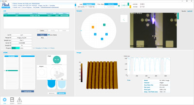
The NX-Wafer is equipped with automated software that makes operation nearly effortless. Just select the desired measurement program to get precise multi-site analysis with optimized settings for cantilever tuning, scan rate, gain, and set point parameters.
Park's user-friendly software interface gives you the flexibility to create customized operation routines so you can access the full power of the NX-Wafer and get the measurements you need.
Creating new routines is easy. It takes about 10 minutes to make one from scratch, or less than 5 minutes to modify an existing one.
Park NX-Wafer’s automated system features:
• Auto, semi-auto, and manual mode so you have complete control
• Editable measurement method for each automated routine
• Live monitoring of the measurement process
• Automatic analysis of acquired measurement data


 Chat Zalo
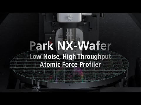

 Đọc thêm